
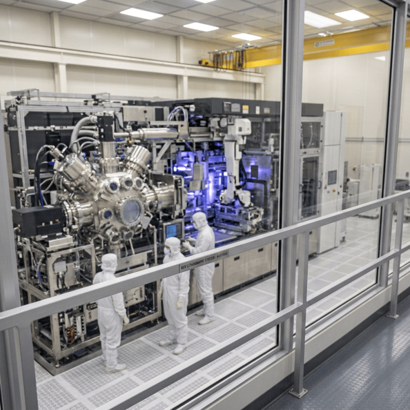
For technology leaders, the real management question is not whether a $400 million tool can print smaller features, but how much strategic dependence the enterprise is willing to accept for that capability. When one supplier, one geography and one equipment class become central to competitive output, procurement becomes a board-level risk conversation, not a routine sourcing decision. CIOs and transformation leaders should treat advanced semiconductor access as a supply-chain resilience issue that sits alongside cost, performance and innovation targets.
The investment trade-off is also changing. Tools like this do not simply improve throughput; they alter the economics of product road maps, partner selection and time-to-market assumptions. That means portfolio leaders need clearer answers to practical questions: Which business units actually benefit from the capability uplift? What revenue or product advantages justify the premium? Where should the enterprise tolerate single-supplier exposure, and where should it keep alternatives alive even if they are slower or less efficient?
There is also an operating-model implication. As fabrication capability becomes more concentrated and capital intensive, internal product teams, procurement, legal, risk and engineering need tighter decision rights on technology commitments. Vendor managers should ask how escalation paths, export constraints, maintenance dependence and upgrade timing are being governed. The next step for executives is to test whether the current roadmap assumes uninterrupted access to this class of equipment—or whether contingency plans exist if geopolitics, lead times or pricing shift again.
Jos Benschop is climbing a ladder to get to the top of his newest machine.
It’s a bit of a schlep. The contraption is the size of a double-decker bus—more than 150 tons of gleaming precision-milled aluminum covered in thousands of snaking tubes, colored cables, and pressurized tanks. From the ground, it looks like a futuristic V8 engine. When I reach the top with Benschop we’re looking down from about 15 feet in the air, with bunny-suited technicians scurrying around below.
It’s more than 200 cubic meters of tech—“mechatronic devices that hold a few mirrors in a position with atomic precision,” he says, gesturing at the gargantuan apparatus. Benschop, a tall and grizzled 66-year-old, has spent over a decade working with his engineers to design this thing, but even so, he’ll sometimes look at it and go: Oh my God.
Benschop is the executive vice president of technology for ASML, a Dutch company that is the linchpin of the microchip industry. If you want to make powerful chips to power phones or AI, a lithography machine like the one we’re standing on is what you need to create increasingly tiny circuitry. Lithography is the art and science of shining light on a silicon wafer to pattern out the transistors, wiring, and other components of the microchips that will be cut from it.
The chipmaking field is essentially controlled by only two big players: ASML, which creates the lithography machines, and TSMC, the chipmaking giant.
Nine years ago, ASML began selling machines that use a daring new way of patterning chip features. These machines employ extreme-ultraviolet light, or EUV—radiation well outside the visible spectrum that they produce by shooting lasers at tiny molten drops of tin, tens of thousands of times a second. Those first machines—the result of an R&D moonshot that lasted 16 years and cost about $10 billion—can craft transistor features with a resolution of 13 nanometers. This new machine can do even better: It has a resolution of just eight nanometers, the width of about 40 silicon atoms. The devices are now shipping to chipmaking factories, or fabs, at an eye-watering price: $400 million each.
But chipmakers will fork that cash over, because they are in a desperate race to produce new and improved chips every year. That means getting their mitts on machines that can make ever smaller components and cram them together ever more densely—part of a long-standing recipe for creating faster and more energy-efficient chips.
For years now, ASML’s tools have been critical to keeping Moore’s Law alive. Without the company’s advanced chipmaking technology it is very possible that chip density—and the ability to perform ever more calculations—would have plateaued.
The AI industry has produced new and ravenous demand for denser chips, as firms like OpenAI and Anthropic scramble to erect server farms that train and deploy new, ever-more-powerful models, which require new, ever-more-powerful hardware. ASML’s latest machine promises to help keep the AI party raging for at least another decade.
“We can allow customers to go to smaller and smaller features, and that opens up the space for whatever we see now today in AI, which is absolutely mind-blowing,” Marco Pieters, ASML’s CTO, told me. “I think we’ve only seen the tip of the iceberg.”
Its relentless push for “shrink”—as they call it in the chipmaking industry—has made ASML a dominant force: The company produces about 90% of all chip-lithography tools worldwide. If you make chips, ASML is unavoidable.
But that monopoly position makes some people, and governments, uneasy. The chipmaking field is essentially controlled by only two big players: ASML, which creates the lithography machines, and TSMC, the chipmaking giant in Taiwan, which uses ASML’s machines to craft the vast majority of all microchips. This duopoly is so powerful that it has geopolitical implications. In an effort to prevent China from developing advanced AI, the US government pressured the Dutch government to impose an embargo in 2019: ASML isn’t allowed to sell high-end machines to any Chinese firm. Geopolitically, “chips are the new oil,” says Marc Hijink, the author of Focus: The ASML Way. Being deprived of them can be as disastrous as being deprived of oil. And in that metaphor, you might say, ASML is the Strait of Hormuz.
James Proud, the cofounder and CEO of the lithography startup Substrate, says the situation is not ideal. The US is “dangerously reliant” on a supply chain that’s overseas and increasingly pricey, Substrate says on its website. “There’s a huge concentration in a small number of players,” Proud says. “And the supply chain is just very expensive.”
Which is why, after two decades of ASML’s dominance, would-be competitors are now gunning for its territory. China is hungrily pouring billions into trying to replicate ASML’s tech. And startups like Substrate are trying to get in the game as well, setting their sights on creating lithography machines that are cheaper, smaller, and even more capable than ASML’s behemoths. Will any of them succeed? The near future clearly belongs to ASML, but as its engineers well know, you can unseat a giant with the right trick of the light.
Making chips is, oddly, a bit like silk-screening a T-shirt. To print a pattern on a silicon wafer, you start with a pattern on a reticle—a mask that carries the design. Shining a light on the reticle transfers that pattern to the wafer. The light interacts with a layer of chemicals on the wafer, fixing the pattern in place.
The size of a chip’s features is partly set by the wavelength of light the machine uses: The smaller the wavelength, the teensier the circuitry you can create. You can stretch the capabilities of a wavelength somewhat; increasing what’s known as the numerical aperture, which usually means swapping in a bigger lens, can further focus the light and thus lay down patterns for smaller and smaller components. Eventually, though, this trick hits its limit, and you need to find a new form of light with a smaller wavelength.
So the history of chipmaking has been a two-step dance. The industry finds a good source of light, eventually increases the numerical aperture, and then finally accepts the need for a smaller wavelength, starting the two-step all over again. Up to the early 1990s, chipmakers used visible light, with a wavelength of about 400 nanometers. By the mid-’90s they’d upgraded to deep ultraviolet, ultimately getting it down to a 193-nanometer wavelength. By the late ’90s they saw the end of the line approaching for deep ultraviolet. But what would come next?
All the options were troublesome. They could shift to x-rays, with a teensy one-nanometer wavelength, but they were devilishly hard to focus. Beams of electrons and ions were equally precise; but they worked like dot-matrix printers, transferring a pattern point by point, which was far too slow. (The chip industry wants a machine to crank out hundreds of wafers per hour.)
“It’s a very engineering-heavy company: Let’s send thousands of engineers and just have them mow down these problems. That’s what they did, and it worked.”
Jeff Koch, analyst, SemiAnalysis
Around 2001, ASML, then a smaller player in the lithography world, placed its bet on another option: EUV, with a wavelength just shy of the x-ray range. Nikon and Canon were working on it as well, but they dropped out—while ASML kept going. The idea was full of unknowns. Nobody knew how to reliably generate that type of light, nor how to focus it; EUV is absorbed by regular glass lenses. It’s even absorbed by air. ASML figured it would take six full years to wade through this R&D nightmare.
In reality it took those 16 years and about $10 billion in research, but it worked. The machine, which works in a vacuum, creates EUV light by vaporizing molten tin and using mirrors to direct it. Zeiss, a historic German optics company, had to invent new techniques for polishing and inspecting the mirrors, using an ion beam to knock off minute imperfections.
“They sort of ignored the buzz of, like, Hey, this is never gonna work, and they just beat their heads against these huge engineering problems,” says Jeff Koch, who used to work for ASML and is now an analyst for the chip-industry research firm SemiAnalysis. “It’s a very engineering-heavy company: Let’s send thousands of engineers and just have them mow down these problems. That’s what they did, and it worked.”
When the first EUV machines went on the market in 2017, they cost well over $100 million apiece. Some observers wondered whether the demand would really be there from the major chipmaking firms—TSMC, Samsung, and Intel. In the years chipmakers were waiting for EUV to happen, the lithography industry had developed clever ways to improve on old-fashioned deep ultraviolet light. (If you put a layer of water on top of the wafer, for example, the light could focus more narrowly.) Maybe EUV wouldn’t be much needed for a while?
But ASML lucked out. Only a few years after EUV debuted, OpenAI released GPT-3 and then ChatGPT. Artificial intelligence burst into the mainstream. Instantly, firms like OpenAI, Google, Meta, and Anthropic were hungry for increasingly high-end chips as they built massive server farms to train and deploy large language models. EUV made it easier and faster to crank out AI-tailored chip designs. Nvidia began producing elite GPUs—processors perfectly suited for AI training—that cost $40,000 a pop; the big companies couldn’t get enough. The AI wars were on, and EUV was in demand. In 2025, ASML says, it sold nearly 50 EUV machines to companies and pulled in nearly $40 billion in revenue. As of press time, the company’s market cap was over half a trillion dollars.
ASML’s new machines have no shortage of potential customers. But there is one in particular, with deep pockets, that can’t buy them for any amount of money: China.
The US wants to hobble China’s ability to create cutting-edge AI chips—or any advanced chips, for that matter. So when ASML began selling its original EUV machines, in 2017, the Trump administration successfully pressured the Dutch government to forbid the company from selling them to any Chinese firms. The US had also imposed export controls on China’s telecom giant Huawei, banning US firms from using its 4G and 5G equipment.
This one-two punch incensed the Chinese government and stirred it to action. China is now pouring billions into catching up and trying to develop its own EUV chip-patterning technology. A Reuters report last winter found that a government skunkworks employing former ASML staffers had cobbled together a machine so huge it filled the entire floor of a lab. It’s unclear how well it works. The experiment may well be making some chips, says Hijink, but he doubts it can do so at an industrial scale.
Officially, the government denied it was pushing to develop EUV tech. An editorial in the Global Times—a newspaper closely allied with the Chinese government—pooh-poohed the report, claiming that China was still happy to work with the West to get access to chips. “Our goal has never been to build a self-sufficient ‘technology island’ in isolation,” it stated, “but rather, on the basis of achieving autonomy and control over key technologies, to integrate more deeply and equally into the global innovation network.”
Experts say the reality is in the middle. China definitely craves a domestic ability to make high-end chips. And unlike ASML, it doesn’t need its EUV machinery to be efficient and profitable, cranking out about 200 wafers an hour. Any output would help wean it off reliance on the West.
“They would be very happy to have a tool that does one wafer per hour and it costs them a fortune to run,” Koch says. “They would build a fab with a thousand of those and be super happy with it.”
Still, producing and managing EUV light well is a feat that might take years, some told me. In the meantime, the Chinese will lean hard on deep-ultraviolet lithography, developed in the ’90s, making the most of an alternative but slower approach known as multi-patterning, says David Lin, senior advisor for tech leadership at the Special Competitive Studies Project, a think tank that focuses on security and technology. “They’re going to push DUV to the absolute limits,” Lin says.
The AI race is also pushing China to devise ever cleverer ways of developing LLMs that don’t rely on the fastest AI chips. In the US, OpenAI, Anthropic, and Google are fighting over who can buy the biggest piles of hot Nvidia chips. Since China can’t compete that way, it is innovating not in hardware but in software—building lighter-weight LLMs like DeepSeek.
As China rumbles into action, ASML has remained laser focused on shrink. To go even smaller, Benschop and his engineers decided, they wouldn’t shift to a new form of light. They’d do the second part of the two-step: They’d raise the numerical aperture of the machine by more than half (for those keeping track of the specific numbers, it would be a switch from an NA of 0.33 to an NA of 0.55). That would let them cut the size of the transistors by close to half and nearly triple their density on a chip.
This would also be an easier climb. Without the need to develop an entirely new source of light, the new machine—based on high-numerical-aperture EUV, or “high NA”—would be evolutionary, not revolutionary.
Still, building the new system did present a few gnarly challenges. In an EUV machine, the way you transfer an image onto a wafer is by shining light at the microchip pattern on the reticle and then using an optical system to take the reflected light and demagnify that pattern, shrinking it down to the size you want on the wafer. The light hits only part of the reticle at any given time, so you quickly move the reticle back and forth to expose every part of the pattern to the light.
Going to a higher numerical aperture meant they could have smaller features on the reticle. But this also meant that some of the light would be arriving at the reticle—and reflecting off it—at a steeper angle.
That’s what caused problems. The pattern on the reticle is three-dimensional, so light arriving at such a steep angle caused shadows—much the way slanted sunlight creates shadows in the Grand Canyon. That stood to diminish the machine’s ability to make clear patterns.
The new reticle moves with acceleration up to 22 g, much faster than in the company’s original EUV machine. “Don’t try to sit on it, because you’ll pass out.”
The solution was to change the pattern on the reticle—along with the way the mirrors took the light and shrank it down to impart the pattern to the wafer. The designs on the reticle would now be twice as long as they were wide—stretched, as it were, in one dimension.
But this design came with its own problems. The changes to the mirrors meant the area on the wafer exposed during a single scan was half the size it was with the original EUV machines, reducing the system’s speed. And ASML couldn’t tolerate any slowdown: Chipmakers were paying it for machines with massive throughput, about 200 wafers an hour.
If one part of the system slowed down, another part would have to speed up. The engineers decided the machine should move the reticle faster, which meant making the entire mechanism lighter and dramatically redesigning it. The new reticle moves with acceleration up to 22 g, much faster than in the company’s original EUV machine. “Don’t try to sit on it, because you’ll pass out,” Pieters told me. The wafer stage moves around faster as well, in tandem with the reticle.
Meanwhile, over in Germany, Zeiss’s engineers were busy designing mirrors to accommodate the higher numerical aperture and asymmetric shaping of the light. The new mirrors would be about twice as large as those in the regular EUV machines, and the projection system, which carries light from the reticle to the wafer, weighed fully 12 tons, seven times more than before. Zeiss built a new robot-assisted production line to handle these ponderous new beasts. The company says they’re the smoothest surfaces they’ve ever made.
At the same time, ASML was working on making its EUV light source even more powerful, to help make the wafer-exposing process go faster. The engineers calculated that they could improve the output of EUV if they hit each tin droplet three times with the laser instead of twice, as they do in the first machine. That meant the already-hectic system of firing tin would need to speed up by 50%. “The lasers just keep getting bigger,” says Alex Schafgans, the head of engineering at ASML in San Diego, where the EUV light source is built.
Indeed, the lasers for a single machine now fill an entire room. After Benschop showed me the massive high-NA device, we walked across the hall and entered a chamber filled with hulking six-foot-tall boxes that were part of the laser system. Peering through tiny windows in the sides of the units, we could see the glowing purple plasma used in creating the laser light.
When high-NA machines began to roll off the assembly line, one company was waiting hungrily: Intel. The company purchased the very first high-NA machine put up for sale, and in the spring of 2024, 300 ASML engineers showed up in Oregon at one of Intel’s fabs to begin assembling and testing it.
“ASML actually put a giant ribbon around one of the boxes,” says Mark Phillips, an Intel fellow who is director of its hardware and lithography solutions, laughing. His team has been testing the machine to see how well it performs; Phillips wouldn’t give details other than to say he’s “very pleased at the rapid pace of tool health.” He also wouldn’t give a date for when Intel would start using it to make chips, though observers say that will likely happen next year. The company plans to ease it in, using it for just a few precision components on a chip and then gradually for more and more.
What’s at stake is a chance to recapture its mojo. Intel was once a silicon powerhouse, designing the most cutting-edge CPUs for computers and servers, and building them in its own fabs. But in the 2010s, the big new markets were mobile-phone chips and GPUs for AI and gaming, and Intel rapidly lost ground. Apple designed its own mobile chips (and had TSMC make them), while Nvidia did the same thing with GPUs. Google began banging out its own TSMC-made AI chips called TPUs in 2015, and soon it was stuffing data centers full of them.
So in 2021 Intel announced a moonshot. It would aggressively begin building out a foundry business, one that would go toe to toe with TSMC. Instead of creating Intel chips, the Intel foundry would manufacture designs for customers like makers of mobile phones and AI chips.
Intel hopes that being the first to wield high-NA technology will give it an edge in the silicon rat race, making it possible to print tiny patterns faster than anyone else.
It could also make things simpler for customers. Over the years, while waiting for EUV machines to emerge, chip designers used multi-patterning to squeeze more life out of the older forms of light. Every chip is made out of layers, which are laid down to make components like the switches and wiring. If you’re working on one of those layers and need to make features tinier than your machine can normally produce, you can break the pattern for that layer up into several patterns and then expose the wafer to them one at a time. This strategy helped chipmakers keep using older (and cheaper) machines while still creating tinier and tinier components. But multi-patterning is a hassle: It’s more challenging to design the complex overlay of patterns, and much slower to print each chip. Designing a chip is far easier if you know you can do “single patterning,” blasting each layer in one go.
Observers say it won’t be easy to build a foundry business that bests TSMC and Samsung on their own terrain. “Leapfrogging is difficult,” Hijink says. But it’s also true that the high-tech world has such a ravening hunger for better chips that Intel could succeed, simply because even TSMC and Samsung can’t fulfill all that need.
“There’s spillover demand, so Intel can survive off that,” Koch says. “It’s not even scraps now. It’s a meal. It may not be the best foundry, but they can make chips, and there’s only three companies that can do that, right?”
TSMC, for its part, seems to be biding its time when it comes to high NA. “TSMC will deploy high-NA EUV when it is mature and ready to deliver maximum benefit to our customers,” the company wrote to MIT Technology Review. Some suspect it won’t use the machines in serious volume until the 2030s. Part of the reason is cost: TSMC is ruthlessly focused on producing chips as cost-effectively as possible, and the high-NA tools are a blistering $400 million each, far more than the previous EUV rigs. And unlike those, the new machines are not a revolutionary leap upward.
“This is like 30% to 50% better in terms of capability,” says Koch, the analyst and former ASML employee. “This is probably the first tool that hasn’t obviously made business sense right away for ASML.”
It’s not that the industry won’t eventually embrace high NA en masse, Koch says. Most companies will need to, if they want to keep going smaller. But TSMC is more likely to push ahead as far as it can go with its existing EUV tools, using onerous multi-patterning to wring as much as it can out of that generation until it absolutely needs to switch.
“The industry has only shifted paradigms when it just absolutely cannot extend—even one more little bit—out of what it’s been doing,” Koch says.
China isn’t the only party looking to upset the current balance of power. The dominance of ASML, and the swelling cost of its tools, is prompting other upstarts too. But instead of trying to replicate ASML’s breakthroughs in EUV, they’re doing an end run—working on lithography tools that use entirely different forms of light. These will be far cheaper, they promise, and just as powerful.
One is Substrate, a San Francisco–based startup. Founded four years ago, it’s working on a tool that uses x-ray light produced by a particle accelerator. X-rays have a remarkably tiny wavelength, making them a potentially powerful way to create minute features.
Particle accelerators have historically been enormous, making them difficult to fit into a chipmaking process. Substrate says it has harnessed decades of scientific improvements in particle acceleration to produce a light source that’s smaller and suitable for mass production.
Last year the company released images showing that it had created fine patterns, which Proud, the CEO, says are only possible now with a high-NA EUV machine. He says Substrate’s goal is to produce chips at scale by 2030.
But Proud doesn’t intend to sell the tools to TSMC or Intel. Indeed, he doesn’t plan to sell them to anyone. Instead, Substrate wants to create its own fab, building chips using its own tools.
“The amount of chips we’re going to need is going to be many orders of magnitude larger than even the wildest projections you have now.”
James Proud, cofounder and CEO, Substrate
The semiconductor industry, Proud argues, needs new approaches, because it’s become too pricey and too centralized. A single fab today can cost $25 billion to build, up from about $5 billion in the 2010s, the company notes. It’s driving the cost of a single wafer full of advanced chips up toward $100,000, Proud says.
“That is, I think, a prohibitive cost,” he says. There also isn’t enough capacity in the supply chain: “It’s relatively slow and hard to flex to the current increase in demands.” He admires ASML’s EUV tooling—it’s “the apex implementation of that technology”—but new approaches are needed.
That’s partly for national security reasons. Proud and his team think it’s too dangerous for the US to rely on foreign supplies. But he also predicts the current AI boom will go into overdrive, creating a massive demand for chips that the existing ASML/TSMC duopoly won’t be able to deliver: “The amount of chips we’re going to need is going to be many orders of magnitude larger than even the wildest projections you have now.”
Substrate predicts it will be able to produce finished wafers at $10,000 a pop—a tenth of where Proud predicts the rest of the industry is heading. Proud says that’s partly because the company’s system will be vertically integrated, so it will control all parts of the chipmaking process, but also because its lithography tooling will be less complex: “We’re able to put together in a sort of simpler package.”
Still, Substrate is playing its cards close to its chest. Unlike ASML, the company isn’t offering nuanced detail on how it generates light, or on how that then translates into making patterns on a wafer.
Substrate’s ambitions give some industry observers pause. Hijink, who thinks it is probably “unachievable and impossible” to simultaneously master both a new form of lithography and high-throughput fab techniques, regards the company’s secrecy as a red flag. “This industry is about open innovation,” he says.
Koch is more impressed by its ambitions and funding. The type of technology it’s pursuing “is really cool,” he says. “It’s interesting.” But “there’s a long road between lab-scale demonstration and high volume,” he adds. “Is this like an imminent disruption to ASML? Probably not.”
Another startup that is aiming to hit the market around the same time as Substrate is Lace Lithography. Based in Norway, it is devising an entirely different approach—one that doesn’t use light at all. Instead, an energized beam of helium atoms is pointed at the pattern on the reticle. When the helium atoms then hit the wafer, the atoms transfer their energy to it, imparting the design to the chip.
The idea dates back a while. Bodil Holst, the CEO, took it up in 2008, when she was a physicist studying the use of atom beams. MIT professor Henry “Hank” Smith, a pioneer in using x-rays for lithography, told her she should explore using atoms as a mechanism for making microchips, because back then he wasn’t sure ASML’s EUV moonshot would work. “Even if it does, we’ll need atoms eventually,” he told her.
Holst did some experiments to investigate the idea further and partnered with a former PhD student—Adrià Salvador Palau, a physicist and expert in machine learning—to found Lace. Like Substrate’s, its tool is completely different from ASML’s massive machinery. The source of the excited atoms “looks a bit like a rocket motor,” says Palau. “It’s very cool.” While EUV’s wavelength is 13.5 nanometers, the helium atoms offer a precision of 0.1 nanometers. The process also requires far less power, and the machine is intended to be far smaller. Holst tells me the company aims to have machines ready to sell to fabs by 2029 or 2030.
“I think everybody’s really looking forward to something that extends a road map beyond light, beyond EUV,” Palau says.
ASML is watching these upstarts with curiosity. Benschop says he can’t assess whether Substrate’s technology will work reliably and affordably, because the company hasn’t explained anything about its processes. But he went to a conference where Holst and Palau did a presentation outlining Lace Lithography’s technology.
“I’m incredibly impressed with how they do it,” he says. The problem, he says, is he doesn’t think the process produces patterns on the wafer that are deep enough to be useful. “I cannot see how they would scale it to a viable volume product,” he told me.
He suspects ASML’s mastery of EUV will keep it on top for the near future. “So far, I have not seen a viable alternative,” he says. He thinks there’s “no serious runner-up” when it comes to volume manufacturing of the most advanced chip generations.
It’s true that major shifts in chipmaking are slow, says Chris Miller, a professor of international history at Tufts University and the author of Chip War, a book about the worldwide struggle for dominance in the industry. “No doubt we’ll eventually have alternatives [to EUV],” he told me via e-mail. “But it’s worth noting that lithography transitions have historically taken years, if not decades.”
ASML’s executives, too, are pondering their future. Benschop expects high-NA technology to dominate chipmaking into the 2030s. Beyond that? The industry has, indeed, tended to shift to a new form of light every decade.
“You may argue it’s time for the next decade,” he told me after we’d stripped off our bunny suits and he was relaxing with a coffee.
But ASML’s executives suspect they can continue to squeeze more capabilities out of EUV by increasing the numerical aperture even further on their existing machine. They’re already toying with a design that would take an NA of 0.55 to an NA of 0.75: “hyper NA.” It could let them pattern wafers with a resolution of six nanometers. They’re also working on standardizing their various optics into a platform of a single size, so customers could order one machine outfitted for either regular EUV, high NA, or hyper NA. If it’s all in the same-sized unit, it would simplify the costs and logistics of integrating each into a fab. If the company goes through with it, Benschop figures, the hyper-NA tool might hit the market seven or eight years from now and be sold in volume during the second half of the 2030s.
For now, the ball is in ASML’s court. “We’re pushing the limits of physics,” Pieters told me. The question now is whether anyone else can push harder.
Clive Thompson is a science and technology journalist based in New York City. He wrote about the development of ASML’s original EUV machine in MIT Technology Review’s 2021 issue on computing.
Enjoyed this article? Sign up for our newsletter to receive regular insights and stay connected.